How does semiconductor doping work?
The fundamental challenge in electronics, before we could build modern devices, was making materials that could switch reliably between conducting electricity well and acting as an insulator. Pure crystalline silicon, the backbone of nearly all modern electronics, is actually a poor conductor at normal operating temperatures. It possesses a natural resistance that prevents the precise control needed for switches and amplifiers. The secret to unlocking its electronic potential lies in a meticulous process called doping, which is the deliberate introduction of specific impurities into the highly ordered crystal lattice of the semiconductor.[1][2][6]
# Intrinsic State
To appreciate doping, we must first understand the state of a pure or intrinsic semiconductor, such as silicon (Si) or germanium (Ge). [1][4] These Group IV elements form crystal structures where every atom shares its four valence electrons equally with four neighboring atoms in strong covalent bonds. [4][6] For electricity to flow, electrons must break free from these bonds and jump across an energy gap—the band gap—to the conduction band. [4] At room temperature, only a small fraction of electrons have enough thermal energy to make this jump, leaving behind an equal number of positively charged vacancies, or "holes," in the valence band. [4] Because the number of free electrons is equal to the number of holes, the material is charge neutral, but its conductivity is too low for practical use in circuits. [1][6]
# Introducing Control
Doping transforms this static, poorly conducting material into an extrinsic semiconductor whose electrical properties can be precisely engineered. [1][6] The process involves adding trace amounts of atoms from different groups in the periodic table to the molten semiconductor material before it solidifies, or by introducing them later via diffusion or ion implantation into the grown crystal. [1][2] The concentration of these dopants is extremely low, often measured in parts per million (ppm) or even parts per billion (ppb) in high-performance microchips, yet this tiny addition drastically changes the material's ability to carry current. [2]
# Donor Impurities
One primary goal of doping is to increase the population of free electrons. This is achieved by introducing donor impurities, which are elements from Group V of the periodic table, such as phosphorus (), arsenic (), or antimony (). [1][4] Silicon atoms possess four valence electrons, but these Group V atoms have five. [1][5] When one of these impurity atoms replaces a silicon atom in the lattice, four of its five valence electrons form the necessary covalent bonds with the neighbors. [4][5]
The fifth valence electron has very little energy holding it to the impurity atom. It requires very little energy, much less than that needed to break a standard silicon-silicon bond, to jump into the conduction band and become a mobile charge carrier. [1][5] Because this impurity atom readily "donates" a free electron, it is termed a donor. [1][4] In this n-type material (where negative carriers are dominant), the majority carriers are the free electrons, while the holes become the minority carriers. [5]
# Acceptor Impurities
The opposite approach creates a material dominated by positive charge carriers, or holes. This is accomplished by introducing acceptor impurities, which come from Group III of the periodic table, such as boron (), aluminum (), or gallium (). [1][4] Group III elements possess only three valence electrons. [4][5]
When an acceptor atom integrates into the silicon lattice, it can only form three covalent bonds, leaving one bond incomplete—this incompleteness is the hole. [4][5] This hole is highly mobile because an adjacent valence electron can easily jump over to fill the gap, effectively moving the hole elsewhere. [4] The impurity atom, having gained an electron from a neighboring silicon atom to complete its bonding structure, now carries a net negative charge, but critically, it accepts an electron from the lattice, hence the term acceptor. [1][5] This process generates an excess of holes, resulting in p-type material, where holes are the majority carriers and electrons are the minority carriers. [5]

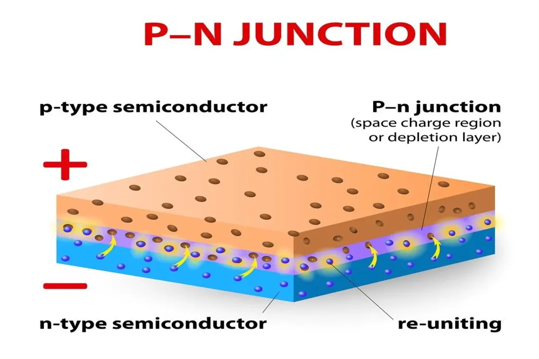
# The Charge Balance Puzzle
A common point of confusion arises when considering the electrical neutrality of doped semiconductors. If an n-type material has a surplus of free, mobile negative electrons, shouldn't the bulk material be negatively charged? The same logic applies to p-type materials having excess positive holes. However, the entire crystal remains electrically neutral overall. [7]
This apparent contradiction resolves when one considers the fixed ionic states of the impurity atoms within the lattice. In n-type silicon doped with phosphorus, once the donor atom gives up its fifth electron, the phosphorus atom itself becomes a stationary, positive ion () locked in place within the crystal structure. [7] This fixed positive charge perfectly balances the mobile negative charge of the donated electron. Similarly, in p-type silicon doped with boron, the acceptor atom captures an electron, becoming a fixed negative ion (), which perfectly balances the charge of the mobile hole it helped create. [7] Doping, therefore, doesn't add net charge to the bulk material; it simply changes the mobility of the existing charge carriers by creating localized, stationary counter-charges within the lattice structure. [5][7]
# Controlling Conductivity Levels
The degree of conductivity is directly proportional to the concentration of the intentionally added dopant atoms. A silicon wafer with acceptor atoms per cubic centimeter () will behave very differently from one with acceptor atoms per cubic centimeter. [2] In very lightly doped materials, the majority carriers come primarily from the dopants, but some thermally generated carriers still exist. As the doping concentration increases, the contribution from the intentionally added impurities overwhelms the natural thermal generation of carriers. [1]
When doping levels become extremely high—approaching the concentration of the host atoms themselves—the material begins to lose its semiconductor nature altogether. At these levels, the distance between impurity atoms becomes so small that their energy levels merge, creating continuous bands similar to those in a metal. This condition is known as heavy doping or degenerate doping, and the material behaves more like a conductor than a semiconductor. [1] Managing this concentration gradient is an engineering feat, as the transition between heavily doped, lightly doped, and intrinsic regions is what allows complex devices like transistors to function by controlling where charge carriers are abundant or scarce. [2][8]
For instance, in fabricating a modern CMOS transistor, specific regions need to be highly conductive to act as the source and drain contacts, while the channel region beneath the gate oxide must be controlled with far greater precision to switch reliably. The ability to control the exact position and concentration of dopants, often achieved through techniques like ion implantation where charged ions are accelerated into the wafer, is what determines the final speed and power consumption of the resulting integrated circuit. [2]

# Beyond Simple Elements
While boron, phosphorus, and arsenic are standard dopants for silicon, other elements and techniques are employed depending on the required material properties. For compound semiconductors, such as Gallium Arsenide (), the doping targets are different. For example, silicon () can be used as an n-type dopant in , while beryllium () is used as a p-type dopant. [1]
Furthermore, there are specialized doping scenarios. For instance, in photolithography steps, sometimes high-energy doping is used to create ultra-shallow junctions. Another scenario involves ion implantation, where dopant atoms are accelerated to high kinetic energy and physically driven into the silicon crystal. While this method offers exceptional spatial control, the violent entry of the ions often damages the crystal structure, requiring a subsequent high-temperature annealing step to repair the lattice and activate the dopants electrically. [2] The success of the entire semiconductor industry hinges on the repeatable, atomic-scale precision of this impurity introduction process, turning an inert element into the foundation of digital information processing. [4]
#Videos
Doping: The Most Important Part of Making Semiconductors - YouTube
Related Questions
#Citations
Doping (semiconductor) - Wikipedia
What is Doping in Semiconductors | WaferPro
The Complete Guide to Doping in Semiconductors - Wafer World
Why and How Do We Dope Semiconductors? - AZoM
Doping: The Most Important Part of Making Semiconductors - YouTube
Doping: n- and p-semiconductors - Fundamentals - Halbleiter.org
why do semiconductors stay neutral after doping? : r/AskPhysics
Doping - PVEducation.org
Doping of Semiconductors - AK Lectures